Semiconductor Class 12 MCQ is one of the best strategies to prepare for the CBSE Class 12 Board exam. If you want to complete a grasp concept or work on one’s score, there is no method except constant practice. Students can improve their speed and accuracy by doing more MCQs on Nuclei Class 12, which will help them all through their board test.
MCQ on Semiconductor Electronics: Materials, Devices and Simple Circuits Class 12 Physics PDF with Answers
Class 12 Physics MCQ with answers are given here to chapter the Semiconductor. These MCQs are based on the latest CBSE board syllabus and relate to the latest Class 12 Physics syllabus. By Solving these Class 12 MCQs, you will be able to analyze all of the concepts quickly in the chapter and get ready for the Class 12 Annual exam.
Learn Class 12 Semiconductor MCQ with answers pdf free download according to the latest CBSE and NCERT syllabus. Students should prepare for the examination by solving CBSE Class 12 Semiconductor MCQ with answers given below.
Question 1. For amplification by a triode, the signal to be amplified is given to
(a) the cathode
(b) the grid
(c) the glass envelope
(d) the anode
Answer
B
Question 2. For an electronic valve, the plate current I and plate voltage V in the space charge limited region are related as
(a) I is proportional to V 3/2
(b) I is proportional to V 2/3
(c) I is proportional to V
(d) I is proportional to V 2
Answer
A
Question 3. When using a triode, as an amplifier, the electrons are emitted by
(a) grid and collected by cathode only
(b) cathode and collected by the anode only
(c) anode and collected by cathode only
(d) anode and collected by the grid and by cathode.
Answer
B
Question 4. When a triode is used as an amplifier the phase difference between the input signal voltage and the output is
(a) 0
(b) p
(c) p/2
(d) p/4.
Answer
B
Question 5. Carbon, silicon and germanium atoms have four valence electrons each. Their valence and conduction bands are separated by energy band gaps represented by (Eg)C, (Eg)Si and (Eg)Ge respectively.
Which one of the following relationships is true in their case?
(a) (Eg)C > (Eg)Si
(b) (Eg)C < (Eg)Si
(c) (Eg)C = (Eg)Si
(d) (Eg)C < (Eg)Ge
Answer
A
Question 6. Choose the only false statement from the following.
(a) In conductors the valence and conduction bands overlap.
(b) Substances with energy gap of the order of 10 eV are insulators.
(c) The resistivity of a semiconductor increases with increase in temperature.
(d) The conductivity of a semiconductor increases with increase in temperature.
Answer
C
Question 7. In semiconductors at a room temperature
(a) the valence band is partially empty and the conduction band is partially filled
(b) the valence band is completely filled and the conduction band is partially filled
(c) the valence band is completely filled
(d) the conduction band is completely empty.
Answer
A
Question 8. C and Si both have same lattice structure; having 4 bonding electrons in each. However, C is insulator whereas Si is intrinsic semiconductor. This is because
(a) in case of C the valence band is not completely filled at absolute zero temperature
(b) in case of C the conduction band is partly filled even at absolute zero temperature
(c) the four bonding electrons in the case of C lie in the second orbit, whereas in the case of Si they lie in the third
(d) the four bonding electrons in the case of C lie in the third orbit, whereas for Si they lie in the fourth orbit.
Answer
C
Question 9. For a p-type semiconductor, which of the following statements is true?
(a) Electrons are the majority carriers and pentavalent atoms are the dopants.
(b) Electrons are the majority carriers and trivalent atoms are the dopants.
(c) Holes are the majority carriers and trivalent atoms are the dopants.
(d) Holes are the majority carriers and pentavalent atoms are the dopants.
Answer
C
Question 10. At absolute zero, Si acts as
(a) non metal
(b) metal
(c) insulator
(d) none of these.
Answer
C
Question 11. In a n-type semiconductor, which of the following statement is true?
(a) Holes are minority carriers and pentavalent atoms are dopants.
(b) Holes are majority carriers and trivalent atoms are dopants.
(c) Electrons are majority carriers and trivalent atoms are dopants.
(d) Electrons are minority carriers and pentavalent atoms are dopants.
Answer
A
Question 12. In a p type semiconductor, the majority carriers of current are
(a) protons
(b) electrons
(c) holes
(d) neutrons
Answer
C
Question 13. If a small amount of antimony is added to germanium crystal
(a) it becomes a p-type semiconductor
(b) the antimony becomes an acceptor atom
(c) there will be more free electrons than holes in the semiconductor
(d) its resistance is increased.
Answer
C
Question 14. Which of the following, when added as an impurity into the silicon produces n type semiconductor?
(a) B
(b) Al
(c) P
(d) Mg
Answer
C
Question 15. When arsenic is added as an impurity to silicon, the resulting material is
(a) n-type conductor
(b) n-type semiconductor
(c) p-type semiconductor
(d) none of these.
Answer
B
Question 16. To obtain a p-type germanium semiconductor, it must be doped with
(a) indium
(b) phosphorus
(c) arsenic
(d) antimony.
Answer
A
Question 17. When n type semiconductor is heated
(a) number of electrons increases while that of holes decreases
(b) number of holes increases while that of electrons decreases
(c) number of electrons and holes remain same
(d) number of electrons and holes increases equally.
Answer
D
Question 18. The increase in the width of the depletion region in a p-n junction diode is due to
(a) forward bias only
(b) reverse bias only
(c) both forward bias and reverse bias
(d) increase in forward current
Answer
B
Question 19. In an unbiased p-n junction, holes diffuse from the p-region to n-region because of
(a) he attraction of free electrons of n-region
(b) the higher hole concentration in p-region than that in n-region
(c) the higher concentration of electrons in the n-region than that in the p-region
(d) the potential difference across the p-n junction.
Answer
B
Question 20. The barrier potential of a p-n junction depends on
(1) type of semiconductor material
(2) amount of doping
(3) temperature
Which one of the following is correct?
(a) (1) and (2) only
(b) (2) only
(c) (2) and (3) only
(d) (1), (2) and (3)
Answer
D
Question 21. In a p-n junction
(a) high potential at n side and low potential at p side
(b) high potential at p side and low potential at n side
(c) p and n both are at same potential
(d) undetermined.
Answer
A
Question 22. The depletion layer in the p-n junction region is caused by
(a) drift of holes
(b) diffusion of charge carriers
(c) migration of impurity ions
(d) drift of electrons.
Answer
B
Question 23. Depletion layer consists of
(a) mobile ions
(b) protons
(c) electrons
(d) immobile ions
Answer
D
Question 24. In a p-n junction diode, change in temperature due to heating
(a) affects only reverse resistance
(b) affects only forward resistance
(c) does not affect resistance of p-n junction
(d) affects the overall V – I characteristics of p-n junction.
Answer
D
Whoever needs to take the CBSE Class 12 Board Exam should look at this MCQ. To the Students who will show up in CBSE Class 12 Physics Board Exams, It is suggested to practice more and more questions. Aside from the sample paper you more likely had solved. These Semiconductor class 12 MCQs are ready by the subject specialists themselves.
Question 25. Application of a forward bias to a p-n junction
(a) widens the depletion zone
(b) increases the potential difference across the depletion zone
(c) increases the number of donors on the n side
(d) decreases the electric field in the depletion zone.
Answer
D
Question 26. In forward biasing of the p-n junction
(a) the positive terminal of the battery is connected to p-side and the depletion region becomes thick.
(b) the positive terminal of the battery is connected to n-side and the depletion region becomes thin.
(c) the positive terminal of the battery is connected to n-side and the depletion region becomes thick.
(d) the positive terminal of the battery is connected to p-side and the depletion region becomes thin.
Answer
D
Question 27. Reverse bias applied to a junction diode
(a) lowers the potential barrier
(b) raises the potential barrier
(c) increases the majority carrier current
(d) increases the minority carrier current
Answer
B
Question 28. In forward bias, the width of potential barrier in a
p-n junction diode
(a) remains constant
(b) decreases
(c) increases
(d) first (a) then (b)
Answer
B
Question 29. Barrier potential of a p-n junction diode does not depend on
(a) diode design
(b) temperature
(c) forward bias
(d) doping density
Answer
A
Question 30. In a junction diode, the holes are due to
(a) extra electrons
(b) neutrons
(c) protons
(d) missing of electrons
Answer
D
Question 31. A semiconducting device is connected in a series circuit with a battery and a resistance. A current is found to pass through the circuit. If the polarity of the battery is reversed, the current drops to almost zero. The device may be
(a) a p-type semiconductor
(b) an intrinsic semiconductor
(c) a p-n junction
(d) an n-type semiconductor.
Answer
C
Question 32. The cause of the potential barrier in a p-n junction diode is
(a) depletion of negative charges near the junction
(b) concentration of positive charges near the junction
(c) depletion of positive charges near the junction
(d) concentration of positive and negative charges near the junction.
Answer
D
Question 33. If a full wave rectifier circuit is operating from 50 Hz mains, the fundamental frequency in the ripple will be
(a) 25 Hz
(b) 50 Hz
(c) 70.7 Hz
(d) 100 Hz
Answer
D
Question 34. An LED is constructed from a p-n junction diode using GaAsP. The energy gap is 1.9 eV. The wavelength of the light emitted will be equal to
(a) 10.4 × 10⁻²⁶ m
(b) 654 nm
(c) 654 Å
(d) 654 × 10–11 m
Answer
B
Question 35. A p-n junction diode can be used as
(a) condenser
(b) regulator
(c) amplifier
(d) rectifier
Answer
D
Question 36. A p-n photodiode is fabricated from a semiconductor with a band gap of 2.5 eV. It can detect a signal of wavelength
(a) 4000 nm
(b) 6000 nm
(c) 4000 Å
(d) 6000 Å
Answer
C
Question 37. Zener diode is used for
(a) amplification
(b) rectification
(c) stabilisation
(d) producing oscillations in an oscillator.
Answer
C
Question 38. A p-n photodiode is made of a material with a band gap of 2.0 eV. The minimum frequency of the radiation that can be absorbed by the material is nearly
(a) 1 × 10¹⁴ Hz
(b) 20 × 1014 Hz
(c) 10 × 1014 Hz
(d) 5 × 10¹⁴ Hz
Answer
D
Question 39. In a p-n junction photo cell, the value of the photoelectromotive force produced by monochromatic light is proportional to
(a) the barrier voltage at the p-n junction
(b) the intensity of the light falling on the cell
(c) the frequency of the light falling on the cell
(d) the voltage applied at the p-n junction.
Answer
B
Question 40. For transistor action, which of the following statements is correct?
(a) Base, emitter and collector regions should have same doping concentrations.
(b) Base, emitter and collector regions should have same size.
(c) Both emitter junction as well as the collector junction are forward biased.
(d) The base region must be very thin and lightly doped.
Answer
D
Question 41. The device that can act as a complete electronic circuit is
(a) junction diode
(b) integrated circuit
(c) junction transistor
(d) zener diode.
Answer
B
Question 42. Metallic solids are always opaque because
(a) they reflect all the incident light.
(b) they scatter all the incident light.
(c) the incident light is readily absorbed by the free electrons in a metal.
(d) the energy band traps the incident.
Answer
C
Question 43. In a p-type semiconductor the acceptor level is situated 60 meV above the valence band. The maximum wavelength of light required to produce a hole will be
(a) 0.207 × 10⁻⁵ m
(b) 2.07 × 10⁻⁵ m
(c) 20.7 × 10⁻⁵ m
(d) 2075 × 10–5 m
Answer
B
Question 44. The manifestation of band structure in solids is due to
(a) Bohr’s correspondence principle
(b) Pauli’s exclusion principle
(c) Heisenberg’s uncertainty principle
(d) Boltzmann’s law
Answer
B
Question 45. The band gap in germanium and silicon in ev respectively is
(a) 1.1, 0
(b) 0, 1.1
(c) 1.1, 0.7
(d) 0.7, 1.1
Answer
D
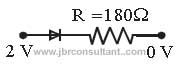
Question 46. A diode having potential difference 0.5 V across its junction which does not depend on current, is connected in series with resistance of 20Ω across source. If 0.1 A current passes through resistance then what is the voltage of the source?
(a) 1.5 V
(b) 2.0 V
(c) 2.5 V
(d) 5 V
Answer
C
Question 47. In a npn transistor 1010 electrons enter the emitter in 10–6 s. 4% of the electrons are lost in the base. The current transfer ratio will be
(a) 0.98
(b) 0.97
(c) 0.96
(d) 0.94
Answer
C
Question 48. Which one is the weakest type of bonding in solids ?
(a) Ionic
(b) Covalent
(c) Metallic
(d) Vander Wall’s
Answer
D
Question 49. The transistor are usually made of
(a) metal oxides with high temperature coefficient of resistivity
(b) metals with high temperature coefficient of resistivity
(c) metals with low temperature coefficient of resistivity
(d) semiconducting materials having low temperature coefficient of resistivity
Answer
A
Question 50. Assuming that the silicon diode having resistance of 20 Ω , the current through the diode is (knee voltage 0.7 V)
(a) 0 mA
(b) 10 mA
(c) 6.5 mA
(d) 13.5 mA
Answer
C
You can easily get good marks If you study with the help of class 12 Semiconductor MCQ. We trust that information provided is useful for you. NCERT MCQ Questions for Class 12 Semiconductor PDF Free Download would without a doubt create positive results.
We hope the information shared above in regards to MCQs on Semiconductor Class 12 with Answers has been helpful to you. if you have any questions regarding CBSE Class 12 Physics Solutions MCQs Pdf, write a comment below and we will get back to you as soon as possible.
Frequently Asked Question (FAQs)
In Class 12 chapter 14 Physics, we have provided 50 Important MCQ Questions, But in the future, we will add more MCQs so that you can get good marks in the Class 12 exam.
Yes, MCQ Question is one of the best strategies to make your preparation better for the CBSE Board Exam. It also helps to know the student’s basic understanding of each chapter. So, You can score good marks in the Class 12 Physics exam.